Applications & Advantages
How innovative Atomic Layer Polishing™ can revolutionize the surface smoothing process
Ultra Smooth Surfaces for Next Generation Semiconductors
Advanced smoothing across multiple surfaces without defects.
No Stress Cracking/Beveling
ALP™
achieves surface quality through atomic level molecular interaction. ALP™
does not bevel wafer outer edges or other structures on the wafer, increasing yield.
Multiple Substrate Smoothing
ALP™ has proven smoothing of 25 key substrates and uses specially formulated and "tunable" chemicals and gasses to achieve ultra-smooth properties.


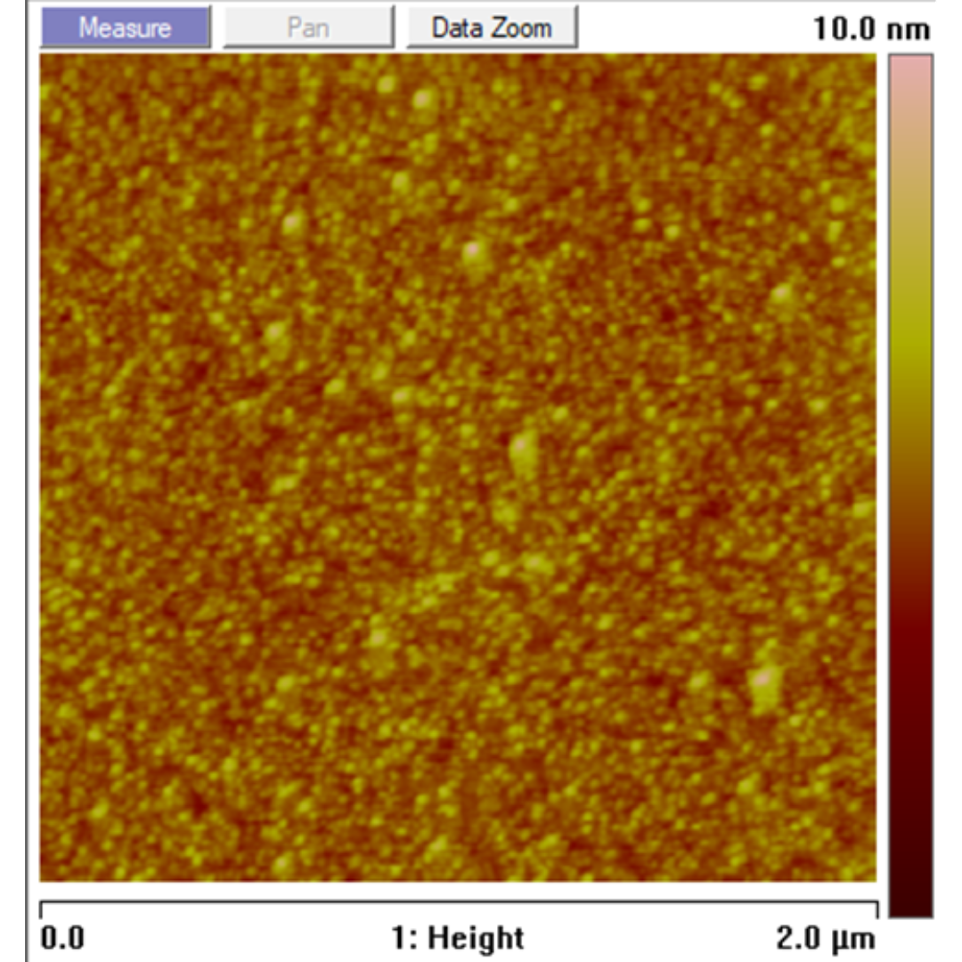
Before ALP™
Gallium nitride (GaN) with an unpolished RMS of 0.60nm.
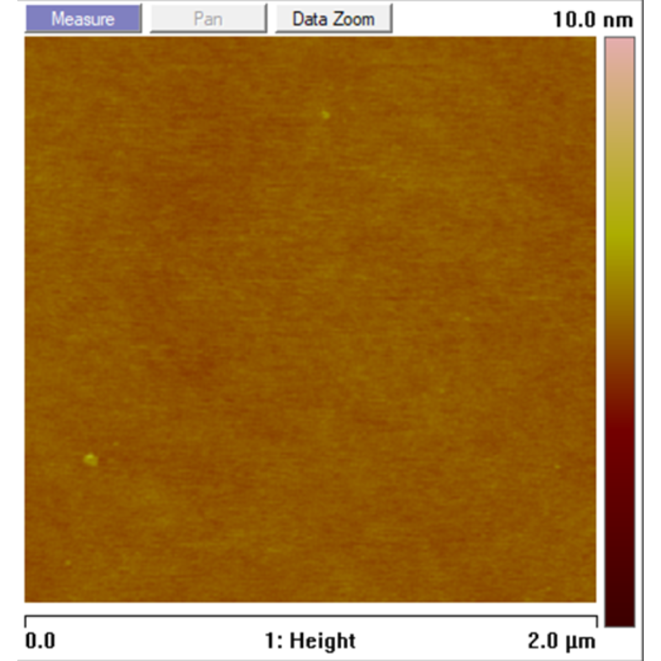
After ALP™
ALP™
delivered a significantly smoother 0.14nm surface finish, polishing with no scratches or debris.